
Description:
Rutherford Backscattering Spectrometry (RBS) is an ion scattering technique that is used primarily for compositional thin film analysis. RBS is unique in that it allows quantification without the use of reference standards and is frequently used to calibrate other analytical methods. It is typically the method of choice for quantitative compositional analysis of thin films used for semiconductors, optical coatings, and other applications where control of film composition is crucial.
TECHNIQUE COMPARISONS
RBS is very complementary to other techniques used for thin film analysis, such as Auger Electron Spectroscopy (AES) and X-ray Photoelectron Spectroscopy (XPS). RBS has lower detection limits than these techniques for heavy elements, but higher detection limits for light elements. Auger offers much better spatial resolution, but can have problems with analyzing insulating samples. XPS can provide chemical state determination in addition to elemental quantification. Both Auger and XPS sample only the upper ~10nm of materials, and use ion beam sputtering to remove material from the sample to obtain a depth profile. This sputtering process can modify the material being analyzed resulting in less accurate quantitative results. RBS does not sputter the sample so it is typically able to provide more accurate quantitative results.
RBS can also be used to non-destructively determine film thickness so it can be used instead o Scanning Electron Microscopy (SEM) or Transmission Electron Microscopy (TEM) cross sectioning. However, in order to derive a film thickness from RBS data one has to assume a density for the film, which leads to an additional source of error. Conversely, if one knows the physical film thickness from another technique such as TEM or SEM then the film density can be calculated using the RBS data. RBS is complementary to X-ray Reflectivity (XRR), which can also determine film density and film thickness but does not determine film composition.
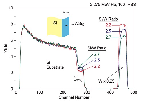
TYPICAL DATA
Figure 1 shows overlaid RBS spectra from WSix films with three different Si/W ratios. The peak at high energy (high channel number) corresponds to scattering from the W in the film while the step at lower energy corresponds to scattering from Si. By measuring the intensities (yield) of the W and Si signals and correcting for the scattering cross sections of W and Si the exact ratio of Si/W can be determined within 1-2%. The width of the W peak is directly proportional to the thickness of the WSix layer. Using known values for the stopping powers of He in W and Si it is possible to calculate the thickness of the WSix layer.
PRINCIPLES
During an RBS measurement, high-energy (MeV) He2+ ions (i.e. alpha particles) are directed onto a sample and the energy distribution and yield of the backscattered He2+ ions at a given angle are recorded. The energies of the backscattered particles depend both upon the mass of atoms from which they scatter (kinematic factor) as well as the depth at which a collision occurs (energy loss factor). The number of backscattered ions is directly proportional to the concentration of a given element. Since the likelihood of a backscattering event is known for all elements (backscattering cross section), it is possible to derive quantitative depth profiles from the RBS spectra for thin films that are less than 1µm thick.
In the case of hydrogen no backscattering occurs, but by placing the sample at a glancing angle to the He2+ ion beam H atoms can be scattered forward out of the sample and collected. This allows the amount of H in thin films to be quantified by using a thin foil to filter forward scattered He atoms, while transmitting only forward scattered H atoms. This separate analysis of H is called HFS (Hydrogen Forward Scattering).
COMMON APPLICATIONS
The ability of RBS to deliver highly accurate film composition without the use of standards makes it ideal for the compositional analysis of semiconductors and other thin films.
Applications include:
- Semiconductor thin film compositional depth profiling:
- Metal silicides: WSi, FeSi, CoSi, TiSi, etc.
- Nitrides: TiN, TaN, TaAlN
- Dielectrics: SiO2, SiN
- High K Dielectrics: HfO2, HfSiO
- Low K Dielectrics: SiOCH
- Compound Semiconductor Layer composition:
- SiGe, AlGaAs, InGaAs, etc.
- Optical Coating compositional depth profiling:
- TiO2, SiO2, HfO2
- Hydrogen in thin films SiO2, SiN, SiOCH, DLC, etc.
- Ion Implant Dosimetry (high Z elements):
- As, Sb, In dose
- Damage profiling in single crystal samples:
- Ion implant, polishing, annealing
STRENGTHS
- Quantitative without the need for reference standards
- Depth profiles of top ~1µm
- Determines film thickness
- Can analyze insulating and conductive samples
- Can measure H, and all other elements except He, Li, Be
- Can analyze full wafers up to 300mm
- Non destructive
LIMITATIONS
- Typically poor detection limits for B, C, N, O (3-5 at-%)
- May not be able to resolve heavier elements of similar mass (e.g., Cu from Zn or W from Ta)
- Smallest analytical area ~2mm diameter
- Sample must be vacuum compatible
 PALS – Positron Annihilation Lifetime Spectroscopy